
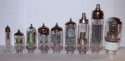
Modern vacuum tubes, mostly miniature style.

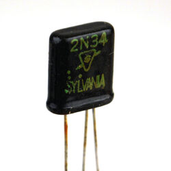
An early 1950s transistor using the precursor to the EIA/JEDEC part numbering system.
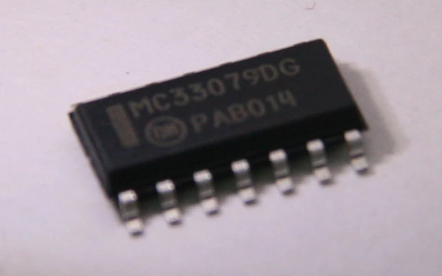
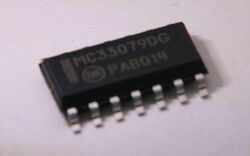
Small-outline integrated circuit. This package has 14 "gull wing" leads protruding from the two long sides and a lead spacing of 0.050 inches.
Terminology
An integrated circuit is officially defined as being:
"A circuit in which all or some of the circuit elements are inseparably associated and electrically interconnected so that it is considered to be indivisible for the purposes of construction and commerce."
Circuits meeting this definition can be constructed using many different technologies, including thin-film transistor, thick film technology, or hybrid integrated circuit. However, in general usage integrated circuit has come to refer to the single-piece circuit construction originally known as a monolithic integrated circuit.
Purpose
Overview
As a smaller alternative to both transistors and valves, as well as a more energy efficient replacement for valves, which had already been proven possible by the growing number of transistors at valves' exspence. The British WW2 Colossus computer was a huge, low bit-rate computer. Custom circuits were made on a add-hock basis using thermionic valves and Thyratrons. It had a total of 1,600 in Mk 1s and 2,400 in Mk 2s, but also relays, fuses, light bulbs, manual switches and electronic stepping switches.
Historical use of valves

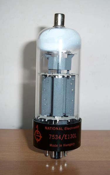
A Hungarian Zapowietrzona E130L Valve. Author:OTLamp.
Colossus was the name of a series of computers developed by British codebreakers in 1943-1945 to help in the cryptanalysis of the Lorenz cipher. Colossus used thermionic valves (vacuum tubes) and thyratrons to perform Boolean and counting operations. Colossus is thus regarded as the world's first programmable, electronic, digital computer, although it was programmed by plugs and switches and not by a stored program.
Colossus was designed by research telephone engineer Tommy Flowers to solve a problem posed by mathematician Max Newman at the Government Code and Cypher School (GC&CS) at Bletchley Park. Alan Turing's use of probability in cryptanalysis contributed to its design. It has sometimes been erroneously stated that Turing designed Colossus to aid the cryptanalysis of the Enigma. Turing's machine that helped decode Enigma was the electromechanical Bombe, not Colossus.
The prototype, Colossus Mark 1, was shown to be working in December 1943 and was operational at Bletchley Park on 5 February 1944. An improved Colossus Mark 2 that used shift registers to quintuple the processing speed, first worked on 1 June 1944, just in time for the Normandy Landings on D-Day. Ten Colossi were in use by the end of the war and an eleventh was being commissioned. Bletchley Park's use of these machines allowed the Allies to obtain a vast amount of high-level military intelligence from radiotelegraphy messages between the German High Command (OKW) and their army commands throughout occupied Europe.
The destruction of the Colossus hardware and blueprints, as part of the effort to maintain a project secrecy that was kept up into the 1970s, when valves finally became obsolete in computrs, deprived most of those involved with Colossus of credit for their pioneering advancements in electronic digital computing during their lifetimes. A functioning replica of a Colossus computer was completed in 2007 and is on display at The National Museum of Computing at Bletchley Park.
A thyratron is a type of gas-filled tube used as a high-power electrical switch and controlled rectifier. Thyratrons can handle much greater currents than similar hard-vacuum tubes. Electron multiplication occurs when the gas becomes ionized, producing a phenomenon known as Townsend discharge. Gases used include mercury vapor, xenon, neon, and (in special high-voltage applications or applications requiring very short switching times) hydrogen. Unlike a vacuum tube (valve), a thyratron cannot be used to amplify signals linearly.
In the 1920s, thyratrons were derived from early vacuum tubes such as the UV-200, which contained a small amount of argon gas to increase its sensitivity as a radio signal detector; and the German LRS Relay tube, which also contained argon gas. Gas rectifiers, which predated vacuum tubes, such as the argon-filled General Electric "Tungar bulb" and the Cooper-Hewitt mercury-pool rectifier, also provided an influence. Irving Langmuir and G. S. Meikle of GE are usually cited as the first investigators to study controlled rectification in gas tubes, about 1914. The first commercial thyratrons didn't appear until around 1928.
A solid-state device with similar operating characteristics is the thyristor, also known as the silicon controlled rectifier (SCR). The term "thyristor" was derived from a combination of "thyratron" and "transistor". Since the 1960s thyristors have replaced thyratrons in most low- and medium-power applications.
In electronics, a vacuum tube, an electron tube, or just a tube (North America), or valve (Britain and some other regions), is a device that controls electric current between electrodes in an evacuated container. Vacuum tubes mostly rely on thermionic emission of electrons from a hot filament or a cathode heated by the filament. This type is called a thermionic tube or thermionic valve. A phototube, however, achieves electron emission through the photoelectric effect. Not all electronic circuit valves/electron tubes are vacuum tubes (evacuated); gas-filled tubes are similar devices containing a gas, typically at low pressure, which exploit phenomena related to electric discharge in gases, usually without a heater.
The simplest vacuum tube, the diode, contains only a heater, a heated electron-emitting cathode (the filament itself acts as the cathode in some diodes), and a plate (anode). Current can only flow in one direction through the device between the two electrodes, as electrons emitted by the cathode travel through the tube and are collected by the anode. Adding one or more control grids within the tube allows the current between the cathode and anode to be controlled by the voltage on the grid or grids. Tubes with grids can be used for many purposes, including amplification, rectification, switching, oscillation, and display.
Invented in 1904 by John Ambrose Fleming, vacuum tubes were a basic component for electronics throughout the first half of the twentieth century, which saw the diffusion of radio, television, radar, sound reinforcement, sound recording and reproduction, large telephone networks, analog and digital computers, and industrial process control. Although some applications had counterparts using earlier technologies such as the spark gap transmitter or mechanical computers, it was the invention of the vacuum tube that made these technologies widespread and practical. In the 1940s the invention of semiconductor devices made it possible to produce solid-state devices, which are smaller, more efficient, more reliable, more durable, and cheaper than tubes. Hence, from the mid-1950s solid-state devices such as transistors gradually replaced tubes. The cathode-ray tube (CRT) remained the basis for televisions and video monitors until superseded in the 21st century. However, there are still a few applications for which tubes are preferred to semiconductors; for example, the magnetron used in microwave ovens, and certain high frequency amplifiers.
Early transistors
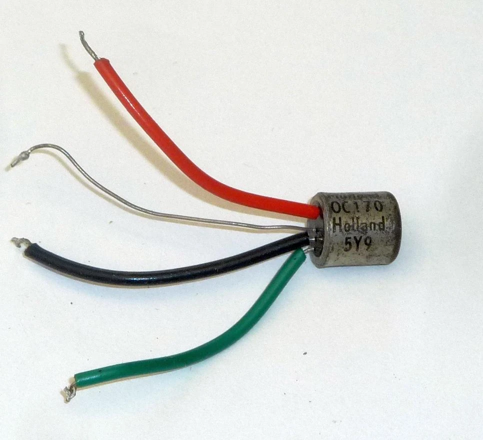
A OC170 germanium PNP alloy junction transistor in TO1 metal case. These were a common transistor in the 1960s for RF and IF stages. This package is noted for a fourth 'shield' connection to the case. These transistors are now decades old and most have failed from the formation of internal metal crystalisation known as 'whiskers' that cause short circuits.
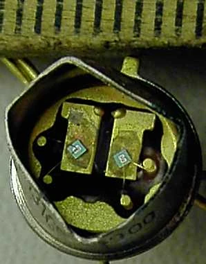
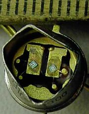
The image shows the transistor chips themselves - 1 by 1 mm. The lines at the top are millimeter spaced. The house they are in are TO39 or TO5 like. Pay attention to the four small bonding wires that are welded on the chips and on the terminals glued in the red-blackish matter. The two small rectangular plates where the chips are placed, are normally the collector terminals. It is not a integrated circuit since the 2 transistors are separate and not united as 1 common chip.
The American 2N34 PNP Germanium Alloy Junction Transistor would lead to cheaper and smaller radios and TVs like the famous American Zenith Royal 500 of the 1950s.
IC overview
An integrated circuit or monolithic integrated circuit (also referred to as an IC, a chip, or a microchip) is a set of electronic circuits on one small plate (also known as a "chip" or a "die") of semiconductor material, normally silicon or germanium. This can be made much smaller than a discrete circuit made from independent electronic components. ICs can be made very compact, having up to several billion transistors and other electronic components in an area the size of a human fingernail. The width of each conducting line in a circuit can be made smaller as the technology advances; in 2008 it dropped below 100 nanometers, and was reduced to 14 nanometers in 2014.
ICs were made possible by experimental discoveries showing that semiconductor devices could perform the functions of vacuum tubes and by mid-20th-century technology advancements in semiconductor device fabrication. The integration of large numbers of tiny transistors into a small chip was an enormous improvement over the manual assembly of circuits using discrete electronic components. The integrated circuit's mass production capability, reliability and building-block approach to circuit design ensured the rapid adoption of standardized integrated circuits in place of designs using discrete transistors.
ICs have two main advantages over discrete circuits: cost and performance. Cost is low because the chips, with all their components, are printed as a unit by photolithography rather than being constructed one transistor at a time. Furthermore, packaged ICs use much less material than discrete circuits. Performance is high because the IC's components switch quickly and consume little power (compared to their discrete counterparts) as a result of the small size and close proximity of the components. As of 2012, typical chip areas range from a few square millimeters to around 450 mm2, with up to 9 million transistors per mm2.
Integrated circuits are used in virtually all electronic equipment today and have revolutionized the world of electronics. Computers, mobile phones, and other digital home appliances are now inextricable parts of the structure of modern societies, made possible by the low cost of ICs.
History
Invention
Early developments of the integrated circuit go back to 1949, when German engineer Werner Jacobi (Siemens AG) filed a patent for an integrated-circuit-like semiconductor amplifying device showing five transistors on a common substrate in a 3-stage amplifier arrangement. Jacobi disclosed small and cheap hearing aids as typical industrial applications of his patent. An immediate commercial use of his patent has not been reported.
The idea of the integrated circuit was conceived by Geoffrey W.A. Dummer (1909–2002), a radar scientist working for the Royal Radar Establishment of the British Ministry of Defence. Dummer presented the idea to the public at the Symposium on Progress in Quality Electronic Components in Washington, D.C. on 7 May 1952. He gave many symposia publicly to propagate his ideas, and unsuccessfully attempted to build such a circuit in 1956.
A precursor idea to the IC was to create small ceramic squares (wafers), each containing a single miniaturized component. Components could then be integrated and wired into a bidimensional or tridimensional compact grid. This idea, which seemed very promising in 1957, was proposed to the US Army by Jack Kilby and led to the short-lived Micromodule Program (similar to 1951's Project Tinkertoy). However, as the project was gaining momentum, Kilby came up with a new, revolutionary design: the IC.
Jack Kilby's original integrated circuit
Newly employed by Texas Instruments, Kilby recorded his initial ideas concerning the integrated circuit in July 1958, successfully demonstrating the first working integrated example on 12 September 1958. In his patent application of 6 February 1959, Kilby described his new device as "a body of semiconductor material … wherein all the components of the electronic circuit are completely integrated." The first customer for the new invention was the US Air Force.
Kilby won the 2000 Nobel Prize in Physics for his part in the invention of the integrated circuit. His work was named an IEEE Milestone in 2009.
Half a year after Kilby, Robert Noyce at Fairchild Semiconductor developed his own idea of an integrated circuit that solved many practical problems Kilby's had not. Noyce's design was made of silicon, whereas Kilby's chip was made of germanium. Noyce credited Kurt Lehovec of Sprague Electric for the principle of p–n junction isolation caused by the action of a biased p–n junction (the diode) as a key concept behind the IC.
Fairchild Semiconductor was also home of the first silicon-gate IC technology with self-aligned gates, the basis of all modern CMOS computer chips. The technology was developed by Italian physicist Federico Faggin in 1968, who later joined Intel in order to develop the very first single-chip Central Processing Unit (CPU) (Intel 4004), for which he received the National Medal of Technology and Innovation in 2010.
Early 3 and later 5 transistor chips
The production of a cheep and efficient early era 3 and later 5 transistor microchip for basic electrical functions. The Plessey SL201 integrated circuit and Philips TAA320 integrated circuit were successful examples from the early 1950s.
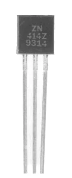
The ZN414 integrated circuit
A ZN414 IC in a TO92 package. Attribution: Nkendrick at the English language Wikipedia.
The idea was the production of a cheep and efficient 5 transistor microchip for basic radio set circuit functions. It was first created in 1972 and became very popular with both business and hobbyists around the world. The ZN414 integrated circuit is a successful example of this radio-chip concept from 1972.
It was chips like this that lead to a lot smaller pocket radios.
The 555 timer IC
The 25 transistor 555 timer IC is an integrated circuit (chip) used in a variety of timer, pulse generation, and oscillator applications. The 555 can be used to provide time delays, as an oscillator, and as a flip-flop element. Derivatives provide up to four timing circuits in one package.
The IC was designed in 1971 by Hans R. Camenzind under contract to Signetics, which was later acquired by Dutch company Philips Semiconductors (now NXP).
Manufacturing
The semi-conductors of the periodic table of the chemical elements were identified as the most likely materials for a solid-state vacuum tube. Starting with copper oxide, proceeding to germanium, then silicon, the materials were systematically studied in the 1940s and 1950s. Today, monocrystalline silicon is the main substrate used for ICs although some III-V compounds of the periodic table such as gallium arsenide are used for specialised applications like LEDs, lasers, solar cells and the highest-speed integrated circuits. It took decades to perfect methods of creating crystals without defects in the crystalline structure of the semi-conducting material.
Semiconductor ICs are fabricated in a planar process which includes three key process steps – imaging, deposition and etching. The main process steps are supplemented by doping and cleaning.
Semiconductor device fabrication is the process used to create the integrated circuits that are present in everyday electrical and electronic devices. It is a multiple-step sequence of photo lithographic and chemical processing steps during which electronic circuits are gradually created on a wafer made of pure semiconducting material. Silicon is almost always used, but various compound semiconductors are used for specialised applications.
The entire manufacturing process, from start to packaged chips ready for shipment, takes six to eight weeks and is performed in highly specialized facilities referred to as fabs.
Mono-crystal silicon wafers (or for special applications, silicon on sapphire or gallium arsenide wafers) are used as the substrate. Photolithography is used to mark different areas of the substrate to be doped or to have polysilicon, insulators or metal (typically aluminium) tracks deposited on them.
Integrated circuits are composed of many overlapping layers, each defined by photolithography, and normally shown in different colors. Some layers mark where various dopants are diffused into the substrate (called diffusion layers), some define where additional ions are implanted (implant layers), some define the conductors (polysilicon or metal layers), and some define the connections between the conducting layers (via or contact layers). All components are constructed from a specific combination of these layers.
In a self-aligned CMOS process, a transistor is formed wherever the gate layer (polysilicon or metal) crosses a diffusion layer.
Capacitive structures, in form very much like the parallel conducting plates of a traditional electrical capacitor, are formed according to the area of the "plates", with insulating material between the plates. Capacitors of a wide range of sizes are common on ICs. Meandering stripes of varying lengths are sometimes used to form on-chip resistors, though most logic circuits do not need any resistors. The ratio of the length of the resistive structure to its width, combined with its sheet resistivity, determines the resistance.
More rarely, inductive structures can be built as tiny on-chip coils, or simulated by gyrators. Since a CMOS device only draws current on the transition between logic states, CMOS devices consume much less current than bipolar devices.
Electrical generations
In the early days of simple integrated circuits, the technology's large scale limited each chip to only a few transistors, and the low degree of integration meant the design process was relatively simple. Manufacturing yields were also quite low by today's standards. As the technology progressed, millions, then billions[18] of transistors could be placed on one chip, and good designs required thorough planning, giving rise to new design methods.
The first integrated circuits contained only a few transistors. Early digital circuits containing tens of transistors provided a few logic gates, and early linear ICs such as the Plessey SL201 or the Philips TAA320 had as few as two transistors. The number of transistors in an integrated circuit has increased dramatically since then. The term "large scale integration" (LSI) was first used by IBM scientist Rolf Landauer when describing the theoretical concept;[citation needed] that term gave rise to the terms "small-scale integration" (SSI), "medium-scale integration" (MSI), "very-large-scale integration" (VLSI), and "ultra-large-scale integration" (ULSI). The early integrated circuits were SSI.
SSI circuits were crucial to early aerospace projects, and aerospace projects helped inspire development of the technology. Both the Minuteman missile and Apollo program needed lightweight digital computers for their inertial guidance systems. Although the Apollo guidance computer led and motivated integrated-circuit technology, it was the Minuteman missile that forced it into mass-production. The Minuteman missile program and various other Navy programs accounted for the total $4 million integrated circuit market in 1962, and by 1968, U.S. Government space and defense spending still accounted for 37% of the $312 million total production. The demand by the U.S. Government supported the nascent integrated circuit market until costs fell enough to allow firms to penetrate the industrial, and eventually, the consumer markets. The average price per integrated circuit dropped from $50.00 in 1962 to $2.33 in 1968. Integrated circuits began to appear in consumer products by the turn of the decade, a typical application being FM inter-carrier sound processing in television receivers.
The first MOS chips were small-scale integration chips for NASA satellites.
The next step in the development of integrated circuits, taken in the late 1960s, introduced devices which contained hundreds of transistors on each chip, called "medium-scale integration" (MSI).
In 1964, Frank Wanlass demonstrated a single-chip 16-bit shift register he designed, with an incredible (at the time) 120 transistors on a single chip.
MSI devices were attractive economically because while they cost little more to produce than SSI devices, they allowed more complex systems to be produced using smaller circuit boards, less assembly work (because of fewer separate components), and a number of other advantages.
Further development, driven by the same economic factors, led to "large-scale integration" (LSI) in the mid-1970s, with tens of thousands of transistors per chip.
SSI and MSI devices often were manufactured by masks created by hand-cutting Rubylith. An engineer would inspect and verify the completeness of each mask. LSI devices contain so many transistors, interconnecting wires, and other features that it is considered impossible for a human to check the masks or even do the original design entirely by hand. The engineer depends on computer programs and other hardware aids to do most of this work.
Integrated circuits such as 1K-bit RAMs, calculator chips, and the first microprocessors, that began to be manufactured in moderate quantities in the early 1970s, had under 4,000 transistors. True LSI circuits, approaching 10,000 transistors, began to be produced around 1974, for computer main memories and second-generation microprocessors.
Stats
| Generational name. | Signification. | Year. | Transistors number. | Logic gates number. |
|---|---|---|---|---|
| SSI. | small-scale integration. | 1964. | 1 to 10. | 1 to 12. |
| MSI. | medium-scale integration. | 1968. | 10 to 500. | 13 to 99. |
| LSI. | large-scale integration. | 1971. | 500 to 20,000. | 100 to 9,999. |
| VLSI. | very large-scale integration. | 1980. | 20,000 to 1,000,000. | 10,000 to 99,999. |
| ULSI. | ultra-large-scale integration. | 1984. | 1,000,000 and more. | 100,000 and more. |
Casing
Also see: IC and transistor in line packaging

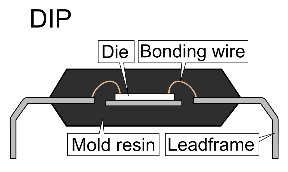
Schematic of a dual in-line package (DIP). Author: Tosaka.
In electronics manufacturing, integrated circuit packaging is the final stage of semiconductor device fabrication, in which the tiny block of semiconducting material is encapsulated in a supporting case that prevents physical damage and corrosion. The case, known as a "package", supports the electrical contacts which connect the device to a circuit board.
In the integrated circuit industry, the process is often referred to as packaging. Other names include semiconductor device assembly, assembly, encapsulation or sealing.
The packaging stage is followed by testing of the integrated circuit.
The term is sometimes confused with electronic packaging, which is the mounting and interconnecting of integrated circuits (and other components) onto printed-circuit boards.
A metal can with epoxy inside sits over the IC that is on a epoxy pad. The legs are metal and attach to the IC with thin gold wires. Some were fully encased in epoxy or in a metal can filled with argon, sand or epoxy. The case is often made of epoxy or plastic, and offers compact size and durability at a very low cost.
Just like vacuum tubes (valves), semiconductor packages standards may be defined by national or international industry associations such as JEDEC, Pro-Electron, or EIAJ, or may be proprietary to a single manufacturer.
Safe handling of ICs
Always earth your self since static electricity can easy burn them out.
Images
")
.jpg "Unijuction transistor KT117 (open).jpg (567 KB)")
")
.JPG "Microchip PIC16C74A die (2).JPG (6.33 MB)")
")
")
")
")
")
Also see
- Science
- Integrated circuits
- Plessey SL201 integrated circuit
- Philips TAA320 integrated circuit
- American 2N34 PNP Germanium Alloy Junction Transistor
- IC and transistor in line packaging
- Dual in-line package (DIP or DIL)
Sources
- http://www.edwardbosworth.com/CPSC2105/Lectures/Slides_06/Chapter_04/MSI_CPSC2105.htm
- https://www.coursehero.com/file/p1ps8lj/Integrated-Circuits-SSI-SSI-Small-Scale-Integration-Early-to-mid-1960s/
- http://www.daenotes.com/electronics/devices-circuits/integrated-circuits-ic
- https://en.wikipedia.org/wiki/Integrated_circuit_packaging
- https://en.wikipedia.org/wiki/555_timer_IC
- http://www.155la3.ru/k145_3.htm#k145hk1
- https://en.wikipedia.org/wiki/Integrated_circuit_packaging
- https://en.wikipedia.org/wiki/555_timer_IC
- http://www.155la3.ru/k145_3.htm#k145hk1
- https://en.wikipedia.org/wiki/Integrated_circuit
- https://en.wikipedia.org/wiki/Semiconductor_package
- https://en.wikipedia.org/wiki/Dual_in-line_package#Single_in-line
- https://en.wikipedia.org/wiki/Integrated_circuit_packaging
- https://en.wikipedia.org/wiki/555_timer_IC
- http://www.155la3.ru/k145_3.htm#k145hk1
- https://news.ycombinator.com/item?id=11694188
- https://en.wikipedia.org/wiki/Soviet_integrated_circuit_designation
- https://en.wikipedia.org/wiki/Integrated_circuit
- https://en.wikipedia.org/wiki/Semiconductor_package
- https://en.wikipedia.org/wiki/Dual_in-line_package#Single_in-line
- http://rk86.com/frolov/
- https://en.wikipedia.org/wiki/Transistor
- http://electronics.howstuffworks.com/transistor.htm
- http://whatis.techtarget.com/definition/transistor
- http://www.101science.com/transistor.htm
- https://en.wikipedia.org/wiki/2N7000
- https://en.wikipedia.org/w/index.php?title=BS170&redirect=no
- https://en.wikipedia.org/wiki/TO-92
- https://en.wikipedia.org/wiki/TO-18
- https://en.wikipedia.org/wiki/Semiconductor_device_fabrication
- https://en.wikipedia.org/wiki/2N107
- http://semiconductormuseum.com/PhotoGallery/PhotoGallery_2N35.htm
- https://en.wikipedia.org/wiki/Thyratron
- https://en.wikipedia.org/wiki/Vacuum_tube
- https://en.wikipedia.org/wiki/Colossus_computer
- http://www.colossus-computer.com/colossus1.html